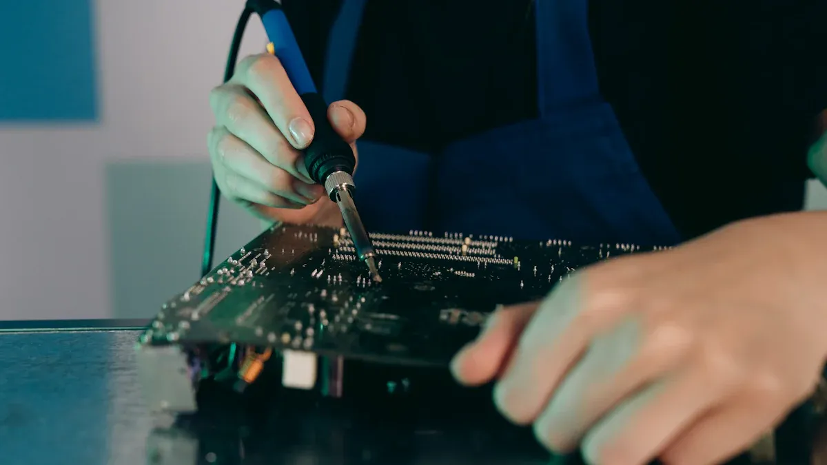
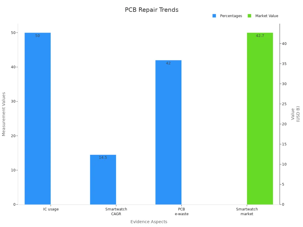
Yes, printed circuit board repair remains possible through proven techniques, specialized tools, and strict safety protocols. Electronics professionals see major benefits from pcb board repair, such as cost savings, reduced e-waste, and longer device lifespans. The industry’s rapid growth—projected to reach $120 billion by 2028—demonstrates the strong demand for repair services. Companies can save up to 50% on replacement costs by choosing pcb board repair instead of full device replacement. AI-powered diagnostics now make pcb repair faster and more efficient, supporting sustainability goals. The table below highlights key market trends driving the importance of printed circuit board repair:
| Evidence Aspect | Statistic / Trend | Implication for PCB Repair and Sustainability |
|---|---|---|
| Increase in IC usage | 50% increase in integrated circuit usage in consumer devices over the last 5 years | Highlights growing electronics demand, emphasizing need to extend device lifetimes and improve recycling |
| Smartwatch Market Size and Growth | Valued at USD 42.7 billion in 2022; CAGR of 14.5% from 2023 to 2032 | Rapid market growth with IC production costs dominating environmental impact, underscoring repair and recycling importance |
| PCB Proportion in E-Waste | PCBs constitute approximately 42% by weight of waste electrical and electronic equipment (WEEE) | Significant portion of e-waste, indicating major opportunity for repair and circular economy approaches to reduce costs and environmental harm |
| Life Cycle Assessment Findings | For low-cost devices like TV remotes, substrate materials contribute most to environmental impact | Suggests repair and use of eco-friendly substrates can mitigate costs and environmental damage |
Technicians who prioritize safety, precision, and quality in every circuit board repair ensure reliable results. Knowing how to repair a circuit board requires understanding modern pcb techniques and using the right tools for pcb board repair.
Key Takeaways
-
Printed circuit board repair saves money, reduces electronic waste, and extends device life, making it a valuable skill for electronics professionals.
-
Technicians must detect common defects like damaged pads, lifted vias, and faulty components early to ensure effective and reliable repairs.
-
Strict safety measures, including ESD protection and organized workspaces, prevent damage to sensitive components and improve repair quality.
-
Using the right tools, such as soldering equipment, inspection devices, and advanced diagnostics, helps technicians perform precise and efficient repairs.
-
Following proven repair techniques and quality control practices ensures durable repairs, supports sustainability, and meets industry standards.
Why Printed Circuit Board Repair Matters
Professional Value
PCB board repair stands as a vital skill for electronics professionals. Many industries rely on circuit board repair to keep devices running smoothly. In custom electronics and the growing IoT sector, technicians use advanced diagnostic tools and precise techniques to restore function. Companies like Soldered Engineering have shown how professional pcb repair services can bring complex smart agriculture devices back to life. These repairs require expertise in soldering, trace repair, and pad repair.
Professional pcb repair services help engineers troubleshoot and maintain modern devices. As technology advances, the need for skilled technicians grows. The electronics industry faces rapid changes and strict regulations. Professionals who master pcb repair support sustainability and device longevity. They use specialized tools and knowledge to diagnose and fix issues quickly. This expertise makes circuit board repair a core competency for anyone working with electronics.
Mastering pcb board repair gives professionals a competitive edge in the fast-changing electronics industry.
Cost and Sustainability
PCB board repair offers major cost savings for businesses and individuals. Replacing a whole device often costs much more than fixing a single circuit board. By choosing circuit board repair, companies can cut expenses and avoid unnecessary waste. Professional pcb repair services also help reduce e-waste, which is a growing problem worldwide. Printed circuit board repair extends the life of devices and keeps valuable materials in use.
Sustainability plays a key role in modern electronics. PCB repair supports green practices by lowering the demand for new materials. Many repair shops now use eco-friendly methods and materials. Electronic circuit board repair helps protect the environment and saves money at the same time. As more people choose pcb board repair, the industry moves closer to a circular economy.
-
PCB board repair reduces landfill waste.
-
Circuit board repair lowers production costs.
-
Professional pcb repair services support environmental goals.
Common Circuit Board Defects
Understanding common circuit board defects helps technicians perform effective pcb repair and maintain device reliability. Early detection and proper repair methods reduce costs and prevent further damage.
Damaged Pads and Traces
Damaged pads and traces often result from improper soldering, thermal stress, or rough handling. These defects appear frequently in high-mix, low-volume production environments. Pad lifting, especially on single-sided pcbs, occurs when copper loses adhesion due to heat or mechanical force. Trained assemblers and automated optical inspection systems help identify these problems before final testing. Preventive measures, such as careful handling and process controls, lower the risk of damage.
-
Damaged pads and traces can interrupt electrical connections.
-
Common causes include excessive heat, poor soldering, and physical stress.
-
Early detection allows for quick circuit board repair and reduces downtime.
Lifted Vias
Lifted vias present another challenge in pcb repair. Vias connect different layers of a circuit board, and lifting usually happens because of thermal cycling or mechanical stress. When a via lifts, it can break the connection between layers, leading to device failure. Technicians must inspect vias closely during circuit board repair. Proper reflow settings and gentle handling during assembly help prevent this defect.
Tip: Always check for lifted vias during visual inspection to ensure reliable pcb performance.
Faulty Components
Faulty components remain a leading cause of pcb failures. These issues include electrical faults, incorrect or obsolete parts, and mismatched footprints. Industry reports show that pcb issues appear 19 times among various failure types, with fuse failures and TVS diode faults also common. Assembly defects, such as poor soldering or wrong components, increase costs and delay repairs. Technicians should verify all parts during circuit board repair to avoid repeated failures.
| Defect Type / Stage | Description / Notes | Frequency Data | Cost Impact / Time to Repair |
|---|---|---|---|
| Missing or Misaligned Parts | Detected by Automated Optical Inspection (AOI) | Common | Minutes to an hour depending on complexity |
| Solder Volume Issues | Includes insufficient solder and solder bridges | Common | Cost increases if detected late |
| Contact-without-Connection Defects | Electrical contact missing despite physical connection | Studied | Cost rises from $0.40 at SPI to $45 at later stages |
| Defect Detection Stages | SPI, AOI, ICT, Final Assembly | Percentages vary | Cost increases by 375% from SPI to AOI, 3000% to Final Assembly |
Early detection and proper pcb repair techniques help reduce costs and improve circuit board reliability.
PCB Board Repair Safety
ESD Protection
Electrostatic discharge (ESD) poses a major risk during pcb board repair. Even a small static charge can damage sensitive pcb components. Technicians must follow strict safety protocols to prevent ESD-related failures. Many repair facilities use a combination of grounding devices, anti-static clothing, and controlled environments to protect circuit boards.
-
Technicians often wear anti-static wrist or heel straps to ground themselves.
-
Conductive floor mats and anti-static smocks help reduce static build-up.
-
Workstations stay grounded, and humidity levels remain between 40% and 70% to limit static electricity.
-
Cleaning with ESD-reducing wipes and using static dissipating tools further lowers risk.
-
The Electrostatic Discharge Association recommends regular testing of all ESD protective equipment to ensure compliance.
-
Proper placement of ESD diodes and careful pcb layout, such as minimizing trace length, also protect sensitive components.
Tip: Always test ESD safety equipment before starting any pcb repair. This step prevents hidden failures and ensures reliable repairs.
Workspace Setup
A well-organized workspace improves both safety and repair quality. Technicians should keep their repair area clean and free of clutter. Good lighting helps spot defects on the pcb. All repair tools must be within easy reach to avoid unnecessary movement.
-
Use ESD-safe mats and wrist straps at every repair station.
-
Store pcb repair tools in anti-static containers.
-
Maintain a dedicated area for cleaning and inspection.
-
Post safety reminders and emergency procedures where everyone can see them.
A safe workspace supports effective pcb board repair. It reduces the chance of accidents and protects both the technician and the pcb. By following these best practices, repair teams can deliver high-quality results and extend the life of every circuit board.
Essential Tools for Circuit Board Repair
Soldering Equipment
Soldering equipment forms the backbone of any pcb repair process. Skilled technicians rely on high-quality soldering irons, hot air rework stations, and precision tips to achieve accurate results. Industry guides highlight several factors that influence efficiency and precision in pcb repair:
-
Certified technicians with steady hand-eye coordination ensure precise soldering.
-
Robust quality control processes maintain repair reliability.
-
Advanced methods, such as BGA pad repair, support high-precision work.
-
Specialized equipment, including temperature-controlled soldering stations, increases accuracy.
Professionals also monitor operational metrics to improve outcomes:
-
Throughput rate measures how many pcb units technicians repair in a set time.
-
Yield rate tracks the percentage of successful repairs, reflecting quality.
-
Downtime analysis identifies periods when soldering equipment needs maintenance.
-
Energy consumption helps evaluate cost-effectiveness during pcb repair.
A reliable soldering setup reduces errors and supports consistent results. Proper solder selection and the use of flux further enhance connection quality.
Inspection Tools
Inspection tools help technicians detect defects before and after pcb repair. Modern inspection methods use both manual and automated approaches. The table below summarizes benchmarks for common inspection tools:
| Method / Study | Dataset Size & Defects | Accuracy | False Positive Rate | Processing Time | Notes |
|---|---|---|---|---|---|
| Bhattacharya & Cloutier (YOLOv5 variant) | 1,386 images, 6 BPCB defect types | 98.3% | <5% | N/A | Custom YOLOv5, data synthesis |
| Ibrahim et al. (XOR template-matching) | N/A | N/A | N/A | ~20 sec | Seven defect types, geometric registration |
| Chaudhary (FAST + MSAC) | N/A | N/A | N/A | ~2.53 sec | Real-time, wire tracks, pads, holes |
| Geometric analysis algorithm | N/A | N/A | N/A | ~2.53 sec | Accurate detection, classification |
High-accuracy inspection tools reduce false positives and speed up the repair process. Visual inspection, magnification, and automated systems all play a role in ensuring pcb quality.
Advanced Tools
Advanced tools take pcb repair to the next level. Technicians use oscilloscopes, multimeters, and logic analyzers to diagnose complex issues. These tools provide detailed insights into voltage, signal integrity, and circuit performance. Soldered Engineering demonstrates how advanced repair tools help restore IoT devices with faulty sensor connections and power supply problems.
Technicians also use micro-soldering, laser repair, and AI-driven diagnostics for miniaturized pcb assemblies. Conductive tapes and custom pads enable repairs in aerospace and industrial settings. Preventive maintenance, such as conformal coating, extends pcb life. The integration of Industry 4.0 technologies, including IoT-enabled diagnostics and augmented reality, further improves repair accuracy and efficiency.
Tip: Investing in advanced repair tools ensures technicians can handle modern pcb challenges with confidence.
Diagnosing Printed Circuit Board Issues
Visual Inspection
Technicians begin pcb troubleshooting with visual inspection. This step helps identify obvious defects before deeper analysis. They use magnifiers, microscopes, and bright lighting to inspect physical components for cracks, discoloration, or missing parts. Visual inspection detects surface anomalies quickly and cost-effectively. Technicians often choose from three types:
-
Direct inspection uses the human eye, sometimes with simple tools.
-
Remote inspection employs devices like borescopes or cameras for hard-to-reach areas.
-
Automated inspection relies on machine vision and AI systems for high precision.
Automated visual inspection stands out for its accuracy. Recent studies show that advanced AI models, such as improved YOLOv5, achieve over 98% accuracy and 99% recall when detecting pcb faults. These systems outperform traditional methods, especially for complex boards. However, visual inspection mainly finds surface defects and may miss hidden issues. Environmental factors and human subjectivity can also affect results.
Tip: Always inspect physical components thoroughly before moving to electrical troubleshooting. This step saves time and prevents missed faults.
Electrical Testing
After visual inspection, technicians use electrical testing to continue pcb troubleshooting. This process helps test individual components and verify circuit integrity. Several protocols support effective troubleshooting and repair:
| Testing Protocol | Description | Effectiveness / Statistics |
|---|---|---|
| Continuity and Isolation Testing | Checks for intact paths and absence of shorts | Essential for signal flow; automated methods improve speed and accuracy |
| In-Circuit Testing (ICT) | Activates every circuit using a "bed of nails" fixture | Detects about 98% of faults; ideal for mass production |
| Flying Probe Testing | Uses probes to test points without custom fixtures | Flexible and low-cost; less effective for large volumes |
| Functional Testing | Simulates real-world conditions to test performance | Uncovers up to 70% of issues; reduces field failures by 30% |
| Solder Joint Inspection | Uses imaging to find solder defects | Reduces failure rates by 40% (IEEE, 2020) |
| Compliance Testing | Ensures boards meet industry standards | Lowers failure rates by 30% (Consumer Electronics Association, 2021) |
Technicians test individual components to confirm proper operation. They use inspection and testing together for thorough pcb troubleshooting. This approach ensures reliable repair and reduces the risk of future failures.
Circuit Board Repair Techniques
Printed circuit board repair requires a combination of skill, precision, and the right tools. Technicians use several proven techniques to restore functionality and reliability. Each method addresses specific defects, from broken traces to faulty components. The following sections outline step-by-step instructions for the most common repair techniques.
Soldering and Desoldering
Soldering and desoldering form the foundation of electronic circuit board repair. Technicians use these methods to attach or remove components, fix broken connections, and correct soldering errors.
Step-by-Step: Soldering a Component
-
Clean the area with isopropyl alcohol to remove dust and residue.
-
Apply a small amount of flux to the pad. Flux improves solder flow and prevents oxidation.
-
Heat the pad and component lead with a soldering iron set to the correct temperature.
-
Feed solder into the joint until it forms a smooth, shiny connection.
-
Remove the iron and allow the joint to cool naturally.
Step-by-Step: Desoldering a Component
-
Heat the solder joint with the soldering iron.
-
Use a desoldering pump or braid to remove the molten solder.
-
Gently lift the component from the board.
-
Clean the pad with alcohol and inspect for damage.
Tip: Always inspect solder joints for cracks, bridges, or cold joints. Proper soldering and desoldering prevent future failures and support reliable circuit board repair.
Pad and Via Repair
Damaged pads and lifted vias can interrupt signal flow on a pcb. Pad and via repair techniques restore these critical connections.
Step-by-Step: PCB Pad Repair
-
Remove any loose or burnt material from the damaged pad.
-
Clean the area thoroughly with alcohol.
-
Apply a small amount of flux to the exposed copper trace.
-
Place a replacement pad or use a conductive adhesive to rebuild the pad.
-
Solder the component lead to the new pad.
-
Inspect the repair under magnification to ensure a solid connection.
Step-by-Step: Via Repair
-
Clean the lifted via and surrounding area.
-
Insert a small wire through the via hole to reconnect layers.
-
Solder both ends of the wire to the appropriate traces.
-
Trim excess wire and secure with epoxy if needed.
Note: Cleaning and flux application are essential for strong, conductive repairs. Always verify continuity with a multimeter after completing pad or via repair.
Trace Reconstruction
Broken or burnt traces disrupt electrical paths on the board. Trace reconstruction restores these connections and prevents device failure.
Step-by-Step: Trace Repair
-
Identify the broken trace using visual inspection and continuity testing.
-
Scrape away solder mask from both ends of the damaged trace to expose copper.
-
Clean the exposed copper with alcohol.
-
Apply flux to the area.
-
Lay a thin wire or copper foil over the gap.
-
Solder both ends of the wire to the exposed copper.
-
Cover the repair with solder mask or epoxy for protection.
| Common Trace Repair Materials | Use Case |
|---|---|
| 30 AWG wire | Fine traces, short gaps |
| Copper foil tape | Wider traces, longer gaps |
| Conductive ink | Quick, low-current fixes |
Callout: Always test the repaired trace for continuity. Proper cleaning and flux use ensure a reliable connection.
Component Replacement
Component replacement stands as one of the most effective repair techniques in electronic circuit board repair. Technicians often encounter faulty capacitors, resistors, or transistors during troubleshooting. Comparative studies show that targeted replacement of faulty components extends the lifespan of PCBs and supports sustainability. This approach reduces costs and waste by addressing specific faults instead of replacing entire boards.
Step-by-Step: How to Repair a Circuit Board by Replacing a Component
-
Gather information about the failure, including user reports and visible symptoms.
-
Inspect the board for obvious damage, such as burn marks or cracked components.
-
Use diagnostic tools like multimeters or oscilloscopes to identify the faulty part.
-
Heat the solder joints and remove the damaged component with tweezers.
-
Clean the pads with alcohol and apply fresh flux.
-
Place the new component on the pads.
-
Solder the leads, ensuring a smooth, shiny joint.
-
Inspect the repair and test the board to confirm proper operation.
Tip: Always use equivalent replacement parts and verify the repair through functional testing. This method supports efficient printed circuit board repair and extends device life.
How to Repair a Circuit Board: Key Points
-
Clean all areas before and after repair.
-
Use flux to improve solder flow and joint quality.
-
Inspect and test every repair to ensure reliability.
Technicians who master these repair techniques deliver high-quality results in electronic circuit board repair. They know how to repair a circuit board efficiently, reduce waste, and support sustainability goals.
Best Practices for PCB Board Repair
Quality Control
Quality control stands at the heart of successful pcb board repair. Leading companies like EMSG and BEST Inc. set high standards by using advanced inspection tools and strict processes. Technicians rely on both contact and non-contact inspection methods to find defects such as missing copper, shorts, or open circuits. Automated Optical Inspection (AOI) and X-ray inspection help reduce defect rates by up to 40% in consumer electronics. In the automotive industry, thermal and vibration testing improve reliability by 30%. Aerospace and defense sectors use cross-sectional analysis and rigorous testing, which can enhance reliability by 50%.
| Industry | Quality Control Methods | Impact on PCB Reliability / Defect Reduction |
|---|---|---|
| Consumer Electronics | AOI, X-ray inspection | 40% reduction in defect rates |
| Automotive | Thermal, Vibration testing | 30% improvement in reliability |
| Aerospace & Defense | Cross-sectional, Rigorous testing | 50% enhancement in reliability |
Technicians also follow strict e-waste regulations, which increase the demand for repair over replacement. Advanced boards with fine lines and ball grid arrays require high technical skill and specialized equipment. Careful inspection and testing after every repair ensure that each board meets industry standards.
Dos and Don’ts
Technicians who follow proven dos and don’ts achieve better results in pcb board repair. These guidelines help maintain quality and prevent common mistakes.
Dos:
-
Preheat the board to prevent thermal shock.
-
Use correct temperature settings and follow international standards.
-
Inspect every repair visually and, when possible, with X-ray tools.
-
Apply solder evenly and with the right amount of pressure.
Don’ts:
-
Avoid disturbing nearby components during repair.
-
Never overheat the board or exceed safe temperature ranges.
-
Do not move components while soldering.
-
Restrict repairs to trained personnel only.
-
Never skip inspection and testing after repair.
Tip: Careful attention to these best practices helps technicians deliver safe, reliable repairs and extends the life of every board.
Proper diagnosis, the right tools, and proven repair techniques help technicians achieve reliable results in printed circuit board repair. Safety and precision remain essential for every repair. Ongoing learning and skill development support better outcomes. Industry professionals use summary metrics to measure success:
| Metric | What It Measures | Why It Matters |
|---|---|---|
| MTTF | Time before failure | Shows device lifespan |
| MTBF | Time between failures | Tracks reliability |
| MTTR | Time to repair | Reduces downtime |
Adhering to industry standards and structured diagnosis extends device life and improves repair quality.
FAQ
What are the most common tools needed for PCB repair?
Technicians often use soldering irons, multimeters, tweezers, and magnifiers. Advanced repairs may require hot air stations or microscopes. Proper ESD protection equipment remains essential for safety.
Can anyone repair a printed circuit board at home?
Trained professionals achieve the best results. Home repairs risk further damage without the right tools or skills. Beginners should practice on scrap boards and follow safety guidelines.
How can someone identify a faulty component on a PCB?
A technician checks for visible damage, discoloration, or bulging parts. He uses a multimeter to test for continuity or shorts. Automated inspection tools help detect hidden faults.
What safety steps should technicians follow during PCB repair?
Always wear an anti-static wrist strap.
Keep the workspace clean and organized.
Use proper ventilation when soldering.
Test ESD equipment before starting any repair.
Is it better to repair or replace a damaged PCB?
| Situation | Recommended Action |
|---|---|
| Minor trace or pad damage | Repair |
| Multiple faulty components | Replace |
| Obsolete or rare boards | Repair |
| Severe physical damage | Replace |
Repair saves money and reduces waste when possible.
Written by Jack from AIChipLink.
AIChipLink, one of the fastest-growing global independent electronic components distributors in the world, offers millions of products from thousands of manufacturers, and many of our in-stock parts is available to ship same day.
We mainly source and distribute integrated circuit (IC) products of brands such as Broadcom, Microchip, Texas Instruments, Infineon, NXP, Analog Devices, Qualcomm, Intel, etc., which are widely used in communication & network, telecom, industrial control, new energy and automotive electronics.
Empowered by AI, Linked to the Future. Get started on AIChipLink.com and submit your RFQ online today!


